My Journey in Designing a LattePanda Mu Mini Carrier
 Yoge2013 2024-07-17 23:45:59 10298 Views8 Replies
 Hi all! Welcome to my project showcasing the journey from concept to working demo: designing a mini carrier board for LattePanda Mu.
If you have any questions, feel free to comment or join the discussion on Discord.
About Me
I'm Yoge, an engineer passionate about electronic hardware design. In my spare time, I enjoy designing and prototyping various circuit boards, finding joy in DIY projects. To date, I have designed multiple boards, including those for 8051, Arduino, RP2040, etc. While I primarily focus on 2-layer board designs, I have begun exploring 4-layer boards as well.
Recently, the release of the LattePanda Mu x86 compute module piqued my interest. Combining this with the need to replace my home's software router, I was inspired to design my own software router, hoping to enhance my hardware design skills in the process.
Project Background
To achieve this goal, I decided to start by designing a simple carrier board to validate the design principles of various interface modules.
Although this was my first attempt at designing such a board, I was pleased to find that all interfaces functioned normally after prototyping and testing. Reflecting on the process, I realized that designing and successfully implementing a carrier board for LattePanda Mu was not as challenging as I had initially thought. With knowledge of some wiring standards, attention to key details, and reference to existing examples, the design can be completed smoothly.
In this article, I will share the design files for this carrier board, along with the key points I have summarized. I hope my learning outcomes will be helpful to fellow community members. I welcome discussion and exchange of ideas in the comments section, where you can share your thoughts and experiences.
Carrier Board Introduction
PCB 3D Photo

Physical Photo

Carrier Board Features
A simple mini carrier board, based on LattePanda's official Lite Carrier with a simplified design.
Main ports include:
- 1x DC Port (12~20V)
- 1x HDMI Port (supports 4K)
- 2x USB 2.0 A Ports
- 2x USB 3.2 Gen2 A Ports (up to 10Gbps)
- 1x Fan Port (4-Pin)
- 1x Power Button with LED
- 1x M.2 E Key 2230 (PCIe x1, USB 2.0, for WiFi module)
- 1x M.2 M Key 2280 (PCIe x1, for NVMe SSD)
Design Software
Due to the large number of capacitors and resistors used on this board, and their small 0402 package size, hand soldering would be extremely challenging.
I typically use JLC PCB for prototyping and SMT. EasyEDA integrates seamlessly with JLC PCB, making it very convenient, which is why I chose to use EasyEDA for this design.
Project Files
Project Files: Please see the attachment in this article.
This project is open-source. You can download the attachment and directly import it into your project. Or, access the above URL and import it into your own project.
Key Points Shared
Board Size
To control costs, I set the board size to 100mm x 100mm.
This is because:
- PCB prototypes within 100mm x 100mm usually enjoy preferential pricing
- Exceeding this size incurs additional engineering fees.
Importance of Signal Trace Uniformity
In high-speed circuit design, a key finding is that signal trace uniformity is more crucial than precise impedance control.
Here's my understanding for reference:
1. Uniformity vs. Precision
- Uniform example: A trace maintaining 100Ω throughout, even if the spec requires 85Ω, can achieve good signal transmission.
- Non-uniform example: A trace with sections at 85Ω, 90Ω, and 95Ω, despite averaging near the target, leads to signal quality degradation.
2. Limitations of Impedance Control Precision
- for instance, JLC PCB offers free impedance control with ±20% accuracy.
- This seemingly low precision is actually not much impactful if traces remain uniform.
3. Manufacturing Considerations
- PCB manufacturing often results in jagged trace edges when you watch the trace under the microscope.
- When these jagged edges are significant relative to trace width, they cause impedance non-uniformity.
- Tip: Avoid using the manufacturer's minimum trace width to ensure better uniformity.
4. Practical Significance of Uniformity
- Uniform traces significantly reduce signal reflection and distortion.
- Even with absolute impedance deviations, uniform traces maintain good signal integrity.
By focusing on trace uniformity, we can significantly improve high-speed circuit performance and reliability without increasing costs. This insight is crucial for optimizing PCB design and enhancing product quality.
PCB Manufacturing Process Selection
Based on the above analysis, I have chosen a relatively safe conventional process to ensure signal line uniformity.
The main selection points are as follows:
- Base Material: FR-4
- Layers: 4
- PCB Thickness: 1.6mm (A thinner option is possible, but given the board's large size, I prefer 1.6mm thickness to prevent bending)
- Outer Copper Weight: 1oz
- Inner Copper Weight: 0.5oz
- Impedance Control: Yes
- Layer Stackup: JLC04161H-7628
- Minimum via hole size/diameter: 0.3mm (Although the design specifications recommend smaller vias, I have found that 0.3/0.5mm vias work well in practice)
Differential Pair Impedance Configuration
Using 90Ω as an example, calculations are performed with the JLCPCB Impedance Calculator. Select Layer Stackup: JLC04161H-7628, set Trace Spacing to 5 mil, and the calculated Trace Width is 8.31 mil.

As mentioned earlier, signal line uniformity is more critical than impedance precision. Therefore, for all functional modules such as HDMI, PCIe, and USB 3.2 Gen2, I've standardized the differential pair impedance control to 90 ohms.
Consequently, the differential pair parameters are set as: Trace Spacing 5 mil, Trace Width 8 mil.

Of course, if you feel that a 5 mil trace spacing is still a bit small, you can certainly set it to: Trace Spacing 6 mil, Trace Width 9 mil.
Differential Pair Spacing Configuration
I use the non coplanar differential impedance. To minimize crosstalk in high-speed interface implementations, the spacing between the signal pairs must be a minimum of 5 times the width of the trace. This spacing is referred to as the 5W rule. Where the high-speed differential pairs abut a clock or a periodic signal, increase this keep-out to a minimum of 50 mils to ensure proper isolation.

In the design rules, set as shown below.

USB 2.0 Routing Roles

USB 2.0 routing is the simplest. You only need to complete the routing by ensuring D+ and D- are equal in width, spacing, and length. Due to the slower speed, the maximum allowable error within the differential pair should not exceed 50 mils.
USB 3.2 Gen1 Routing Roles

USB 3.2 Gen2 Routing Roles

The LattePanda Mu's USB lane specification is USB 3.2 Gen 2.
For detailed USB Routing Roles, please check the link below. The document provides a thorough explanation and you'll find it informative.
Renesas USB3.0 Board Layout Guideline
TI High-Speed Interface Layout Guidelines
PCIe Routing Roles

Note: The above specifications do not apply to PCIe 4.0 and PCIe 5.0.
The M.2 M key and M.2 E key on the carrier board use PCIe signal lines.
For detailed PCIe Routing Roles, please check the link below. The document provides a thorough explanation and you'll find it informative.
Philips PCIe PCB Layout Guideline
Board Design Guidelines for PCI Expres Architecture
HDMI Routing Roles

For detailed HDMI Routing Roles, please check the link below. The document provides a thorough explanation and you'll find it informative.
Length Matching Roles

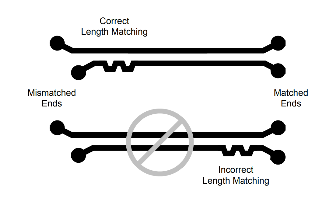
When performing length compensation in a differential pair, start from the source: begin the tuning at the exact point where the mismatch occurs.

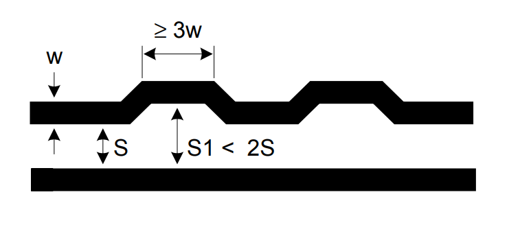
When performing length compensation, matching the length takes priority over impedance values.
However, for protruding line segments: the maximum spacing must be less than twice the normal spacing, and the length must be at least three times the line width.
Corner Routing Roles

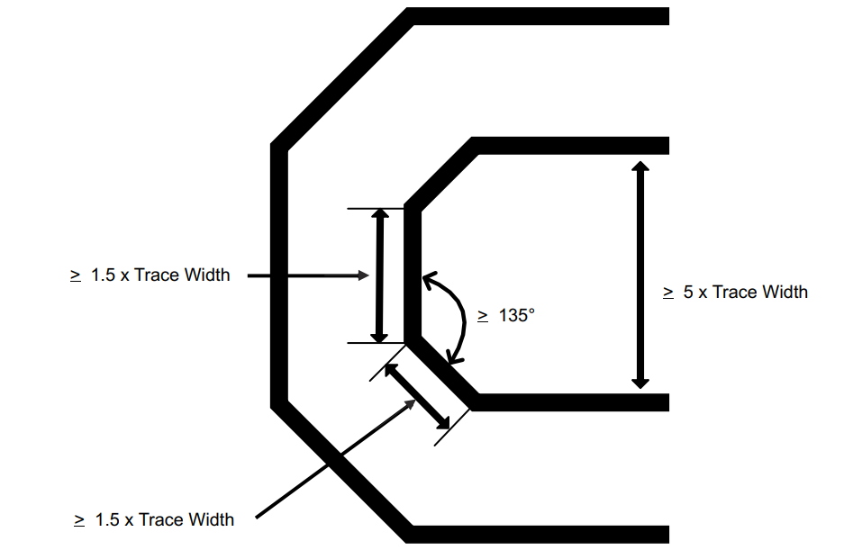
When a differential pair turns, each segment of the inner signal trace at the bend must be at least 1.5 times the trace width.
Layer Transition Roles

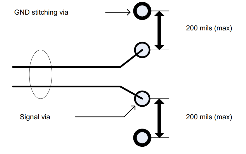
When a differential pair requires layer changes through vias, two return vias (GND vias) must be placed near the signal vias. However, using four GND vias is even better.
* This article will continue to be updated.Thanks!

